

Scientific Innovation
Within the SEP project, we pursue an integrated approach combining multi-scale theory, targeted materials synthesis, and detailed characterization for our project to address these main topics:
- Multi-scale theory
- Synthesis FeS2-, Cu2S-, and CuO-based NC bulk homojunction solar cells
- Synthesis of Zn3P2 and CZTS-based HHDJ solar cells
- Materials and device characterization
Photovoltaic devices operate on the basis of charge-separating interfacial topologies that can be either planar junction (e.g., ci-Si and thin-film inorganic semiconductors) or so-called bulk heterojunction (e.g., OPV). We believe that success in developing economically viable, earth-abundant solar cells will require innovative approaches and concepts. Our team found that cooperation between the heterojunction and the homojunction in the hetero-homo dual junctions (HHDJ) device model enables good performance for CdTe (Cadmium Telluride) and CIGS (Copper Indium Gallium Selenide) solar cells. In order to test the proposed approach, we are pursuing the following two types of solar cells:
- Bulk homojunction for FeS2-, CuxS-, and CuO-based solar cells
- Hetero-homo dual junction concept for Zn3P2- and CZTS-based thin-film solar cells
Zn3P2 films made by Closed-Space Sublimation
Zinc phosphide (Zn3P2) is an earth-abundant semiconductor possessing many properties of an ideal absorber layer for solar cells: long minority carrier diffusion length, high visible light absorption, and a band gap near 1.5 eV. We synthesize Zn3P2 thin films by close-spaced sublimation.
Cu2ZnSnS4 (CZTS) films made by Spray Pyrolysis
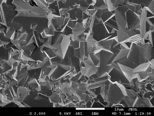
Cu2ZnSnS4 (CZTS) is an earth-abundant semiconductor comprising of non-toxic elements. It has a band gap of ~1.5 eV and an absorption coefficient of 104 cm-1. Recent research outside of UT has yielded CZTS devices with up to ~11 % efficiency. The SEM image above shows single-phase CZTS thin films fabricated by ultrasonic spray pyrolysis.
CZTS nanoparticles made by colloidal synthesis
Literature “one pot” synthesis UT’s injection method
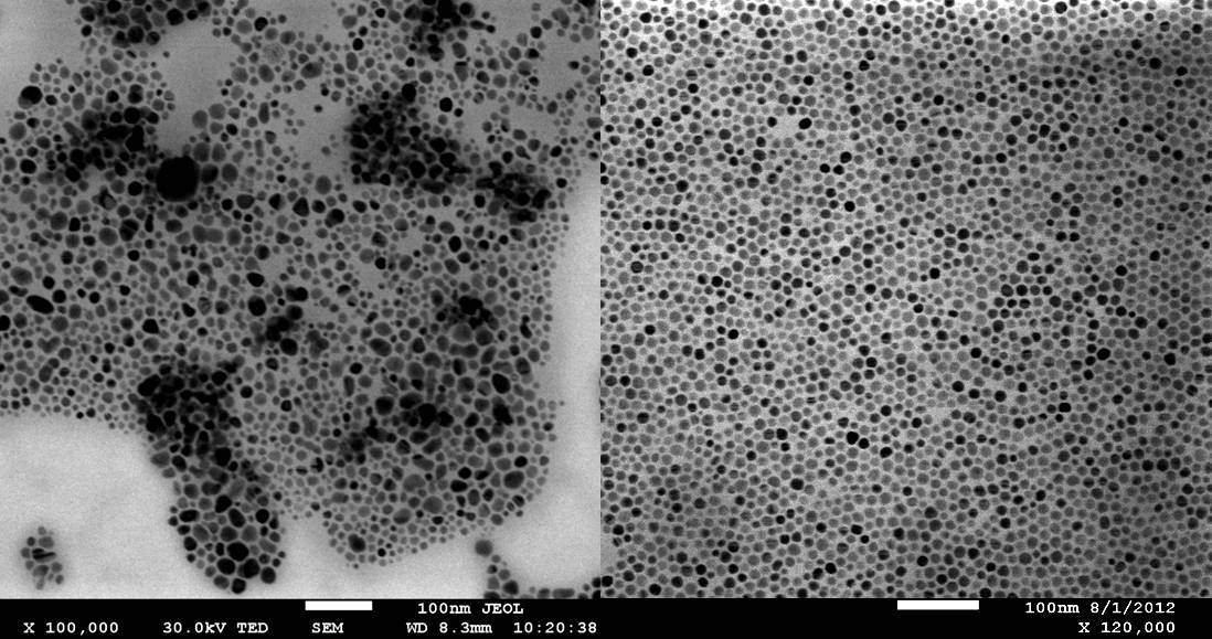
We have also developed colloidal synthesis approaches to making CZTS nanocrystals, in an effort to produce starting material with improved stiochiometry control, and to investigate potential bulk homojunction characteristics. UT’s recent work on synthesis shows significant improvement in size uniformity, as seen above.
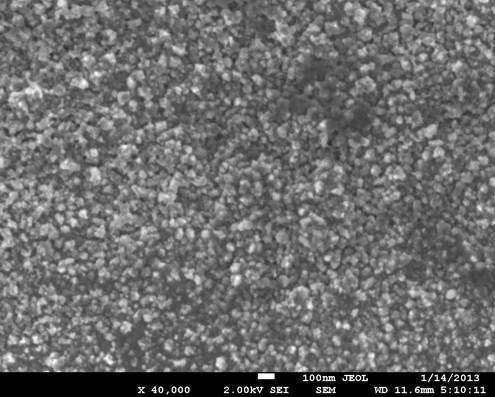
FeS2 Nanocrystals for Thin Film Photovoltaics
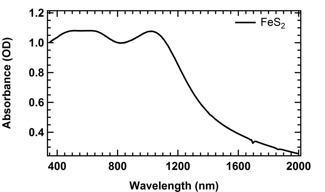
Iron sulfide (FeS2), also known as pyrite, offers another promising though challenging route to affordable solar electricity generation. The bandgap energy of FeS2 is ~1.0 eV, falling very close to the ideal bandgap range of 1.1-1.5 eV for a single-junction PV device. Although many groups have studied FeS2, challenges related to material defects have yielded only relatively low PV conversion efficiency of < 3%. Our work seeks to establish very high quality nanocrystal quality of pyrite in order to use as a building block for highly-controlled thin film stoichiometry and defect density. The above graphs show cubic pyrite and the corresponding optical absorption spectrum.
In2S3 window layer and all-sprayed devices
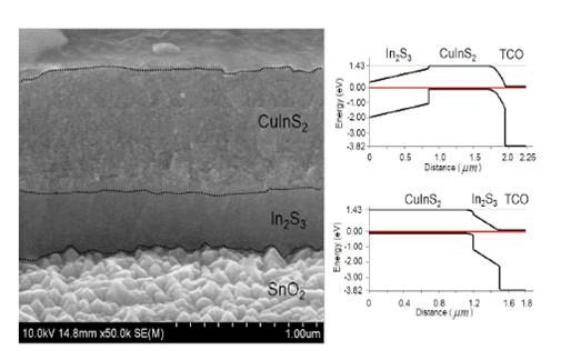
Solutions containing semiconductor nanoparticles and molecular semiconductor precursors can be processed into films by spraying, dipping, or printing. Here we shows a cross-sectional SEM of a TEC 15/In2S3/CuInS2 device prepared by spraying (left) and a calculated band diagram for the layers arranged in two different ways. In2S3 is a non-toxic potential replacement for CdS in several PV devices.